Scanning Electron Microscopy Services
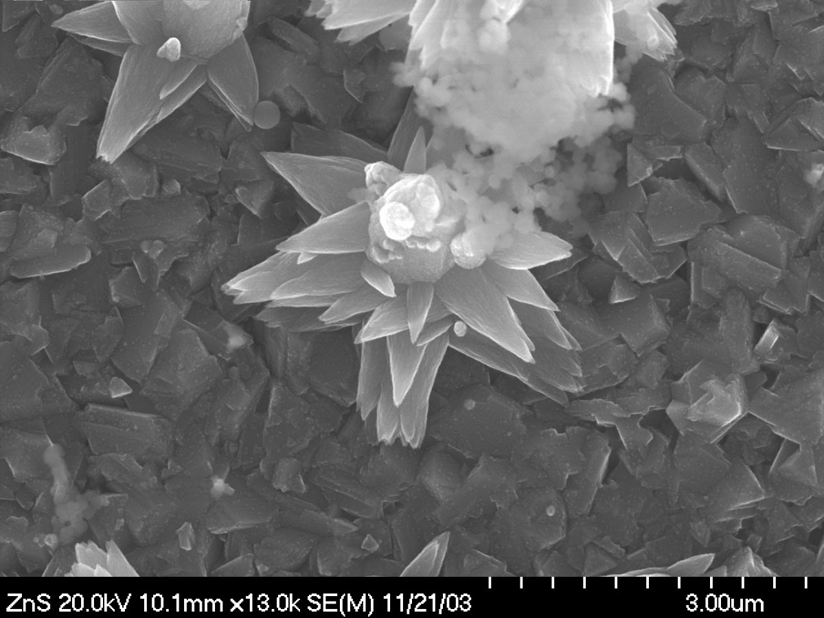 Zinc selenide crystals on polycystaline Copper Indium Gallium Diselenide (CIGS) thin film. |
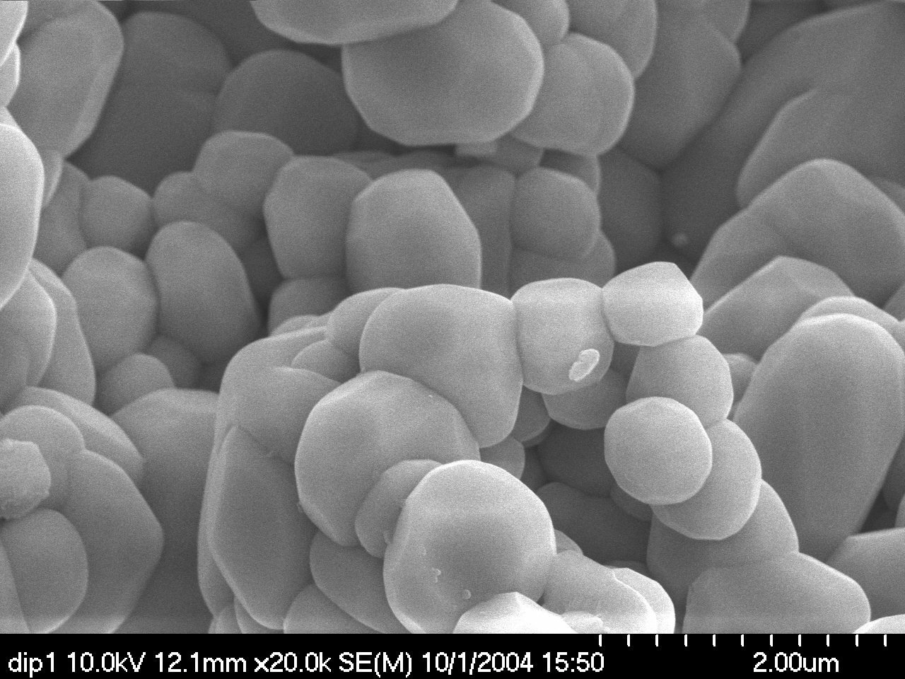 Aggregated Yitrium Aluminum Garnet (YAG) particles. |
Morphology:
The invention of the scanning electron microscope (1937-1965) brought about a new era in microscopy. Objective microscopes had significant limitations in both maximum resolution as well as depth of field. Both were overcome by utilizing electrons instead of photons for imaging to great effect.Scanning electron microscopy (SEM) has now become an industry standard procedure for most samples studied, regardless of further analysis techniques employed. SEM is also a very versatile technique, giving a clear morphological picture of the sample being measured with large depth of field as well as affording the chemical analysis of samples by using their characteristic x-ray radiation emitted upon measurement.
Characteristic X-Ray Analysis (EDS/EDX):
 Every atom bombarded by electrons is imparted with more energy that is dissipated in a number of ways (phonons, photons, auger electrons, etc.)
By utilizing the emitted x-ray photons, characteristic emissions can be used to determine composition of the analyzed samples through energy-dispersive X-ray spectroscopy (EDS/EDX).
EDS mapping is also possible (rastering of the e-beam commensurate with x-ray characteristic wavelength analysis) to produce a map of compositions to overlay with earlier morphological results.
Composition does not need to be known before measurement.
Every atom bombarded by electrons is imparted with more energy that is dissipated in a number of ways (phonons, photons, auger electrons, etc.)
By utilizing the emitted x-ray photons, characteristic emissions can be used to determine composition of the analyzed samples through energy-dispersive X-ray spectroscopy (EDS/EDX).
EDS mapping is also possible (rastering of the e-beam commensurate with x-ray characteristic wavelength analysis) to produce a map of compositions to overlay with earlier morphological results.
Composition does not need to be known before measurement.
Electron Backscatter Diffraction (EBSD):
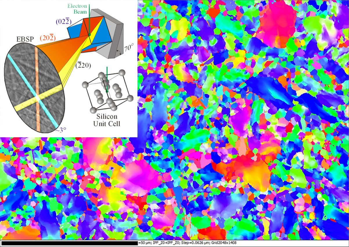 Along with the characteristic X-rays, the sample also emits backscattered electrons. These electrons are diffracted by the atomic structure of crystalline materials.
The emitted Kossel cones and resulting pattern (EBSP) can be used with modeling to determine the orientation of the crystal in free-space.
Crystal orientation, relative crystal disorientation (misorientation) can easily be determined.
EBSP mapping can be performed on complex samples to produce a detailed view of polycrystalline orientations within the samples and determine texture of the material.
EBSP is a useful tool for quick analysis of sample orientations and disorientations, and can be used as supportive information for further X-ray Diffraction (XRD) analysis.
Along with the characteristic X-rays, the sample also emits backscattered electrons. These electrons are diffracted by the atomic structure of crystalline materials.
The emitted Kossel cones and resulting pattern (EBSP) can be used with modeling to determine the orientation of the crystal in free-space.
Crystal orientation, relative crystal disorientation (misorientation) can easily be determined.
EBSP mapping can be performed on complex samples to produce a detailed view of polycrystalline orientations within the samples and determine texture of the material.
EBSP is a useful tool for quick analysis of sample orientations and disorientations, and can be used as supportive information for further X-ray Diffraction (XRD) analysis.
Cathodoluminescence (CL):
Cathodoluminescence is the emission of light (luminescence) from the surface of a material upon the application of cathode rays (an electron beam) to the material. Any material which exhibits catohodluminescence may be analyzed in CL, most frequently, semiconductors and minerals are observed. On example is in the field of photovoltaics. The intensity of emission from photovoltaic absorber layers has been shown to be related to photovoltaic conversion efficiency, making this method useful to track down non-radiative defects.Analytical Capabilites Beyond Imaging:
Thermo Electron state-of-the-art EDS and WDS X-ray Microanalysis System with atmospheric thin window EDS detector and high performance WDS parallel beam spectrometer with hybrid X-ray optics
HKL Technology EBSD System with high resolution camera for crystallographic measurements, high speed texture mapping, and phase identification. Forward Scatter Detector for crystallographic contrast imaging
Gatan MonoCL3 Cathodoluminesence(CL) Spectrometer and imaging system for 300-1700nm. Liquid He Cooled stage module.
Major Specifications:
Resolution 1.2nm (30kV) , 1.5 nm (15kV), 3.0 nm (1kV) imaging performance 3.0 nm (15 kV, 10 mm, 5nA) for high resolution analytical performance
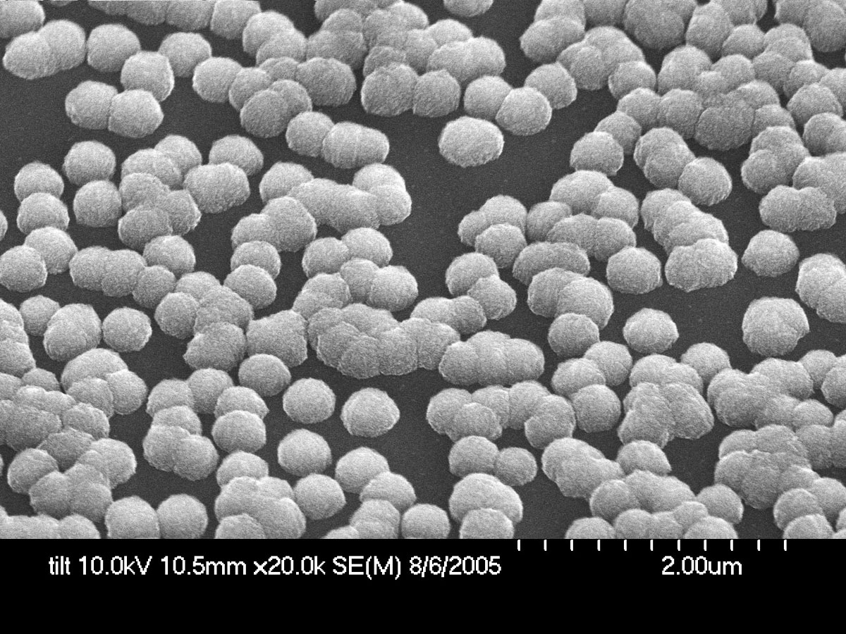
Synthetic diamond balls
Contact us to discuss your characterization needs.
Home || Industry Support || Research Support || Education Support || Contact
Atomic Force Microscopy || X-Ray Analysis || Scanning Electron Microscopy
Prairie Nanotechnology, 60 Hazelwood Drive, Champaign, IL 61820
Phone: 708-406-9608, Fax: 815-301-3851
Email us at: info@prairienanotech.com
This website and its contents © 2015 Prairie Nanotechnology, LLC. All Rights Reserved.